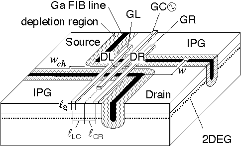
Fig 1. Schematic diagram of the double gate single electron transistor. A single and a coupled quantum dot are formed by applying relevant voltages to the Schottky gates.
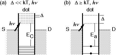
Fig. 2. Energy diagram of the PAT through a dot in the classical Coulomb blockade regime (a), and in the quantum dot regime (b).
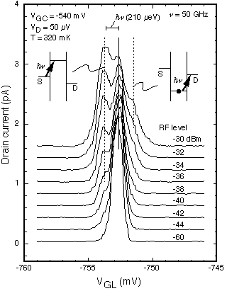
Fig. 3. A Coulomb oscillation peak and PAT current peaks through a quantum dot. Each curve is offset by 0.2 pA for clarity.
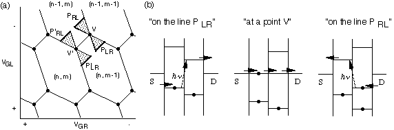
Fig. 4. (a) Schematic charging diagram of the coupled dot system. (n, m) corresponds to the number of electrons in the left dot and in the right dot, respectively. The resonant 0D-0D tunneling peaks are observed at the vertices, V and V'. The thick lines, PLR, PRL, etc., indicate the conditions for the resonant 0D-0D PAT. (b) Energy diagram of the PAT for the condition on the line PLR, at the point V, and (d) on the line PRL.
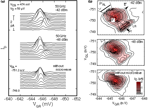
Fig. 5. (a) The drain current profile near the condition V' with and without applying microwave radiation. (b) The contour plot of the current profile. A part of the charging diagram is also attached on the top of the plot. The arrows indicate that E = (E_R + E_L)/2 and e = E_R - E_L are changed.
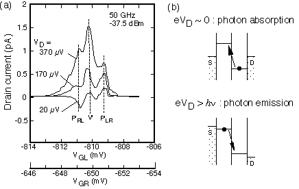
Fig. 6. (a)The drain current profile with a main resonance peak at V' and satellite PAT peaks on P'LR and P'RL. (b) Schematic diagram for the photon absorption and stimulated emission processes