Semiconductor wafer 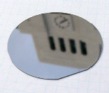 A high-mobility two-dimensional electron system (2DES) can be realized
in an AlGaAs/GaAs modulation-doped heterostructure. A typical wafer consists
of a GaAs cap layer, an AlGaAs doping layer, an AlGaAs spacer layer, a
GaAs channel layer, and buffer layers grown on a GaAs substrate. These
high-quality atomically-smooth layers are grown by Molecular Beam Epitaxy
(MBE) technique. Various nanodevices, such as quantum dots, quantum wires,
quantum point contacts, and edge channels, can be fabricated from an MBE
wafer. [photo: 2" GaAs wafer] A high-mobility two-dimensional electron system (2DES) can be realized
in an AlGaAs/GaAs modulation-doped heterostructure. A typical wafer consists
of a GaAs cap layer, an AlGaAs doping layer, an AlGaAs spacer layer, a
GaAs channel layer, and buffer layers grown on a GaAs substrate. These
high-quality atomically-smooth layers are grown by Molecular Beam Epitaxy
(MBE) technique. Various nanodevices, such as quantum dots, quantum wires,
quantum point contacts, and edge channels, can be fabricated from an MBE
wafer. [photo: 2" GaAs wafer] |
Photolithography system 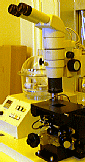 Photolithography is used to fabricate patterns greater than a few microns.
We have a MIKASA spin coater [MS-A100] and a photo-mask aligner [M1-S]
system to transfer photomask patterns to the resist layer on a semiconductor
wafer. After spreading a resist layer on a substrate, ultraviolet light
is exposed through a glass photomask. The irradiated resist layer will
be removed after development. The resist pattern can be used for the lift-off
process and the etching process. Photolithography is used to fabricate patterns greater than a few microns.
We have a MIKASA spin coater [MS-A100] and a photo-mask aligner [M1-S]
system to transfer photomask patterns to the resist layer on a semiconductor
wafer. After spreading a resist layer on a substrate, ultraviolet light
is exposed through a glass photomask. The irradiated resist layer will
be removed after development. The resist pattern can be used for the lift-off
process and the etching process. |
Direct-write photolithography machine (MicroWriter ML3) 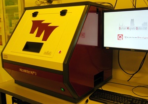 This maskless photolithography machine is used in patterning a resist layer
on a semiconductor wafer. The wafer is exposed to UV light from an LED
through a digital micromirror device with a resolution of 1 micron. The
exposures are repeated with high accuracy to make a large pattern. No mechanical
contacts to the wafer and are required. We use a PMGI sacrificial layer
and an S18xx photoresist layer for lift-off process. We use our home-made
program 'DXF-arranger' to arrange multiple DXF source files to generate
a single CIF file for several photolithography processes. This maskless photolithography machine is used in patterning a resist layer
on a semiconductor wafer. The wafer is exposed to UV light from an LED
through a digital micromirror device with a resolution of 1 micron. The
exposures are repeated with high accuracy to make a large pattern. No mechanical
contacts to the wafer and are required. We use a PMGI sacrificial layer
and an S18xx photoresist layer for lift-off process. We use our home-made
program 'DXF-arranger' to arrange multiple DXF source files to generate
a single CIF file for several photolithography processes. |
Electron beam lithography / Proximity effect correction 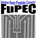 Electron beam lithography is used to fabricate fine patterns less than
100 nm. We can utilize a JEOL EB system at TokyoTech through NanoNet program. Electron beam lithography is used to fabricate fine patterns less than
100 nm. We can utilize a JEOL EB system at TokyoTech through NanoNet program. We have a home-made proximity effect correction program [FuPEC], which adjusts the dose of the electron beam for meshed regions. This is essential for writing complicated patterns with dense and sparse regions. The FuPEC program converts DXF data into J01 format with ShotRank modulation. [test result] [LabReport(日本語)] |
Vacuum evaporator with electron beam and resistance heater 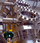 Metal electrodes (gate electrodes or Ohmic contacts) can be fabricated by depositing Au/Ti or AuGeNi alloy on a wafer. Our vacuum evaporator [K-Science] is equipped with an electron beam gun (3 melting pots) and a resistance-heating tungsten boat. A sample holder can be tilted and rotated during the evaporation. The vacuum chamber can be evacuated below 1E-6 Pa by using a turbo molecular pump (550L/s) and a rotary pump (250L/min). Metal electrodes (gate electrodes or Ohmic contacts) can be fabricated by depositing Au/Ti or AuGeNi alloy on a wafer. Our vacuum evaporator [K-Science] is equipped with an electron beam gun (3 melting pots) and a resistance-heating tungsten boat. A sample holder can be tilted and rotated during the evaporation. The vacuum chamber can be evacuated below 1E-6 Pa by using a turbo molecular pump (550L/s) and a rotary pump (250L/min). |
Draft chamber for chemical processes 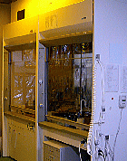 Two draft chambers for acid and organic materials are used for chemical
processes, such as wet chemical etching, surface cleaning, developments
in photo- and EB-lithography processes. Ventilation, scrubber and gas absorption
units are equipped for clean and safety operation. Two draft chambers for acid and organic materials are used for chemical
processes, such as wet chemical etching, surface cleaning, developments
in photo- and EB-lithography processes. Ventilation, scrubber and gas absorption
units are equipped for clean and safety operation. |
Manual Probe Station 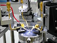 This laboratory-made low-cost manual probe station MPS1000 is designed to measure current-voltage characteristics and microwave characteristics of nanodevices at room temperature. Fabricated nanodevices are screened by testing at room temperature. This laboratory-made low-cost manual probe station MPS1000 is designed to measure current-voltage characteristics and microwave characteristics of nanodevices at room temperature. Fabricated nanodevices are screened by testing at room temperature. Details can be found here. See recent model in WS page [prober] [scriber]. |
Manual wire bonding (West Bond) 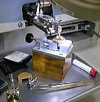 Nanodevices are usually mounted on a specially-designed microwave sample holder with external circuits (if required), and electrical connections are made by wire bonding. Typically 25um gold wire is used for the purpose. Ultrasonic power is introduced to the capillary to make a wire bonding to the bonding pad of the sample. For better microwave transmission, the sample is mounted next to the end of coaxial cables. |
Variable Temperature Insert (VTI) with 9T magnet The VTI Insert (Cryo Inductories of America) is used for low-temperature electrical measurement at variable temperature ranging from 1.5K to 300K. A superconducting magnet (Cryo Magnetics) is used to generate a magnetic field up to 9T. We use this cryostat to investigate fundamental transport characteristics as well as microwave transport. |
Helium 3 Cryostat with 12/14T magnet 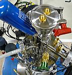 Oxford Helium3 cryostat Heliox is used to measure DC and RF characteristics
of nanodevices at a low temperature below 300 mK. The cryostat is easy
to handle, and the hold time exceeds 90 hrs (by the specification). Two
coaxial cables are installed to feed high-frequency signals to the sample.
The sample can be placed in a shielding box with RF filters. The cryostat
is equipped with 12T superconducting magnet. Oxford Helium3 cryostat Heliox is used to measure DC and RF characteristics
of nanodevices at a low temperature below 300 mK. The cryostat is easy
to handle, and the hold time exceeds 90 hrs (by the specification). Two
coaxial cables are installed to feed high-frequency signals to the sample.
The sample can be placed in a shielding box with RF filters. The cryostat
is equipped with 12T superconducting magnet. |
Dilution refrigerator with 10/12T magnet 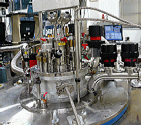 Oxford Kelvinox HA400 [HA: HighAccess option, Nominal cooling power: 400uW]
provides precise electrical measurement at extremely low temperatures (7
mK min.). It has a large space at 4K, 1K, 50mK, and MC (mixing chamber)
plates for cryogenic circuits like cold amplifiers (4K) and passive components.
We have 6 coaxial cables (made of Niobium) for high-frequency measurements
and 24 twisted-pair cables (48 wires) for standard dc measurement. Electromagnetic
noise is filtered by RC filters and copper powder filters. The cryostat
is equipped with a 10/12T superconducting magnet. Oxford Kelvinox HA400 [HA: HighAccess option, Nominal cooling power: 400uW]
provides precise electrical measurement at extremely low temperatures (7
mK min.). It has a large space at 4K, 1K, 50mK, and MC (mixing chamber)
plates for cryogenic circuits like cold amplifiers (4K) and passive components.
We have 6 coaxial cables (made of Niobium) for high-frequency measurements
and 24 twisted-pair cables (48 wires) for standard dc measurement. Electromagnetic
noise is filtered by RC filters and copper powder filters. The cryostat
is equipped with a 10/12T superconducting magnet. |
Cryogen-free (dry) dilution refrigerator with 12T magnet Oxford TRITON [Nominal cooling power: 400uW@100mK] is useful for long-term electrical measurement without supplying liquid Helium. Various cold electronics can be placed in the large-space plates (400mmφ) at 50K, 4K, and base temperature. |
Microwave and pulse generators 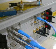 We have strong specialty on high-speed high-frequency measurements for studying quantum dynamics and coherent dynamics. Typical equipments are We have strong specialty on high-speed high-frequency measurements for studying quantum dynamics and coherent dynamics. Typical equipments are- Anritsu high-speed pulse pattern generator (12.5 GHz, 2ch, photo) - Microwave generator (20GHz) - Vector network analyzer (20 GHz) - Sampling oscilloscope (50GHz) with TDR (Time domain reflectometry) module (20 GHz) - Tektronics arbitrary wave generator (10GS/s, 2ch). - Spectrum analyzer (32 GHz) The product of the minimum time resolution (< 0.1 ns) and the thermal energy (<10ueV below 100mK) can be smaller than the Planck's constant (4.14 ueVns), where quantum mechanical characteristics of electrons may appear. |
Cryogenic electronics Some electronic circuits (usually, passive components) need to be operated at low temperatures (<100mK). We designed and fabricated impedance matched copper powder filter, thin coaxial cable for filtering higher-order mode, DC block, LC resonators for impedance transformer, and so on. |
Low-noise DC measurement system 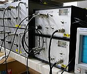 Low-noise measurement is crucial to measure quantum mechanical behavior
in semiconductor nanostructures. Low-noise measurement is crucial to measure quantum mechanical behavior
in semiconductor nanostructures. The 16 channel 16bitx2 DAC unit (left) provides stable DC voltages (10V, 5V, 2V full scale) with 22.5-bit resolution. The current amplifier with optical isolation amplifier (right) is designed to measure small current (approx. 20 fA/sqrtHz). Matsuda precision DAC system - 16 channel (galvanically isolated to each other) - Output: Triaxial connector (or BNC connector for a common reference) - Output voltage range: ±10V, ±2V, ±1V selectable on the front panel - Resolution: coarse 16 bit + fine 16bit for each channel - 1LSB(coarse) = 300uV, 1LSB(fine) = 3 uV in ±10V range - Noise level: 50nV/srootHz at 10Hz (output = 0 V) - Noise level: 1uV/srootHz at 10Hz (output = 10 V) - thermostatic chamber inside (negligible temperature drift) - long-term stability: ±20uV for 7 days with temperature variation from 20 to 30 degree - no clock circuits in the front-end circuit - optically isolated from the interface (GPIB) |
LabVIEW automated program FMA 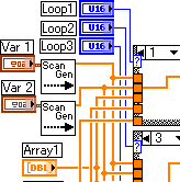 FMA (Flexible Measurement and Analysis) software library allows us to control various instruments through GPIB interface, accumulate measurement data in a file format '.fma', and analyze the stored data in many ways. Each data file involves a three-dimensional array of measured values and measurement conditions (Var1 and Var2). The measurements can be repeated with other conditions for overnight or weekend experiments. FMA (Flexible Measurement and Analysis) software library allows us to control various instruments through GPIB interface, accumulate measurement data in a file format '.fma', and analyze the stored data in many ways. Each data file involves a three-dimensional array of measured values and measurement conditions (Var1 and Var2). The measurements can be repeated with other conditions for overnight or weekend experiments. |
Helium recovery monitor Liquid helium is a refrigerant for low-temperature experiments. We have to recycle Helium to run experiments at low cost. Our home-made Helium recovery monitor watches the Helium recovery rate and the purity continuously, and alert the users via e-mail if the recovery rate becomes low. Daily, weekly, monthly charts of Helium recovery data are available from the web. Typical recovery rate in our lab. is 95-96%. The recoverd helium will be liquified at the Research Center for Low Temperature Physics at TokyoTech. |
Sketch book  The first thing you need to start with is to make a rough sketch of your
idea. Interests in nanoscience, theoretical considerations, sample fabrication,
measurement schemes, experimental details, and so on... These ideas can
be brushed up by rewriting the sketch many times and by discussions with
colleagues, students, and professors. For the purpose, FujisawaLab original functional pen is useful. The first thing you need to start with is to make a rough sketch of your
idea. Interests in nanoscience, theoretical considerations, sample fabrication,
measurement schemes, experimental details, and so on... These ideas can
be brushed up by rewriting the sketch many times and by discussions with
colleagues, students, and professors. For the purpose, FujisawaLab original functional pen is useful. |